Stress (\sigma) is the amount of force being applied to an object per unit of cross-sectional area. If the cross-sectional area varies along the force axis, the smallest area is used. The unit of stress is \unit{Pa} (\N\m^{-2}).
Strain (\epsilon) is the amount of deformation in a material, expressed as the relative change in length (absolute change in length \Delta L over the original length L_0). It is dimensionless.
Elastic deformation is a temporary change to the shape of a material due to applied stress. The material returns to its original shape once the stress is removed.
Plastic deformation is a permanent change to the shape of a material. The material does not return to its original shape after the stress is removed. The amount of stress required before plastic deformation occurs is called the yield stress, yield strength, or \sigma_y. The yield stress of titanium is 820\unit{GPa} and of aluminium is 240\unit{MPa}.
Poisson’s ratio \nu is a measure of how much deformation a material experiences perpendicular to the applied force (transverse deformation) when stretched or compressed (axial deformation). The \nu of most metals is around 0.3, and of most polymers is around 0.5.
The strength of a material is the amount of stress it can withstand before some limit is reached.
Yield strength is the amount of stress a material can withstand before it experiences plastic deformation. This is equal to the stress at the yield point. For most metals a precise yield point cannot be determined, so the 0.2% proof stress is used instead (found by tracing a line upwards from the 0.2% strain point with gradient E).
Ultimate tensile strength (UTS) is the amount of stress a material can withstand before fracturing. This is equal to the stress at the apex of a stress-strain graph. In a brittle material, this is also equal to the yield strength, because brittle materials will fracture instead of plastically deforming.
The toughness of a material is the total amount of energy (work) per unit volume that it can dissipate/absorb before fracturing. Toughness is given by the total area underneath a stress-strain graph between the origin and the fracture point, and is measured in joules.
Ductility is the amount of plastic deformation that occurs in a material before fracturing, measured as either percentage elongation or percentage reduction in area. Ductile materials tend to be tough, but not strong, and will form a ‘cup and cone’ shape when fractured.
A material is brittle if it experiences no plastic deformation before fracture. The resultant fragments can be collected and slotted back together without any gaps. Examples of brittle materials are ceramics and glass. Brittle materials tend to be strong, but not tough.
Fracture is the point where one piece of material becomes many. A gap is often formed in the material at the point of fracture due to sudden recovery of elastic deformation.
Hardness is the resistance of a material to localised plastic deformation.
The indentation test is used to determine the hardness of a material. To perform the test, an indenter of a harder material than the one being tested is pressed into the material using a known force, and then the indentation created is measured. The smaller the indent, the harder the material.
Hardness is related to strength because the material must be plastically deformed in order to leave an indentation, and plastic deformation can only be performed by exceeding the yield strength of the material. Hardness is usually proportional to strength for isotropic materials (properties are uniform in all directions).
There are many different Rockwell scales used for hardness testing, using different indenters and different loads. Each scale measures from 0 to 100. Measured values can’t be compared across scales. Geologists use the Moh’s scale instead, which measures from 1 to 10.
Stress is tightly related to strain. A stress-strain graph plots the amount of strain experienced by a material as an increasing tensile stress is applied.
The initial strain in a material is due to elastic deformation. This elastic portion of the graph is a straight line, with the Young’s modulus E of the material being the gradient of this line (measured in Pascals). A steep slope indicates a stiffer material (steel, glass), and a shallow slope indicates a more elastic material (polyethylene). The Young’s modulus of titanium is 100\unit{GPa}, and of aluminium is 70\unit{GPa}.
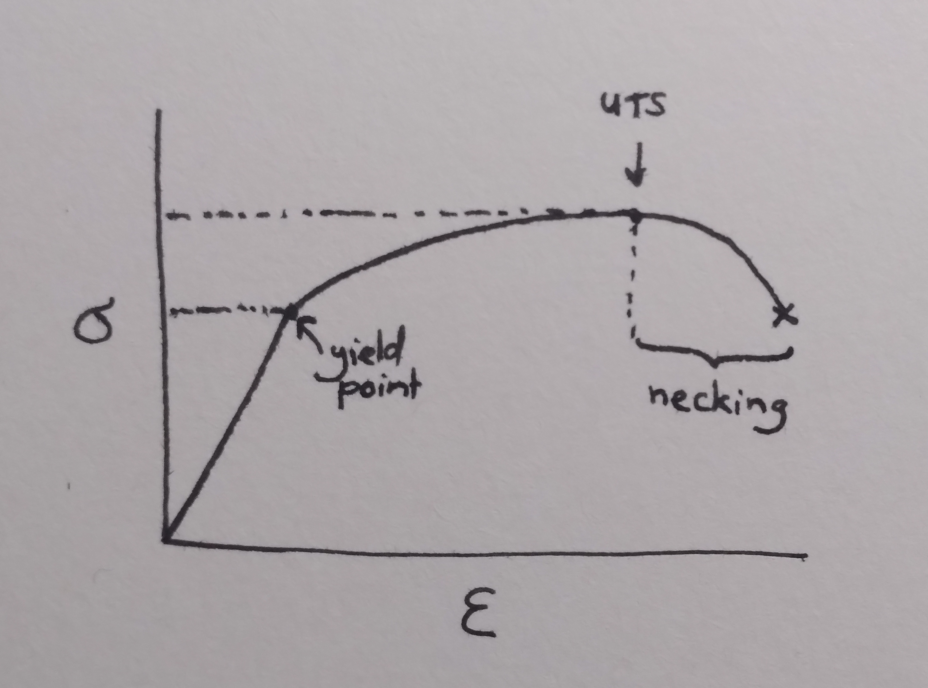
The yield point of a material is represented by a change in the gradient of the stress-strain graph. This is the point where the material stops undergoing further elastic deformation and begins to undergo plastic deformation. The stress at this point is called the yield stress (\sigma_y). If a precise yield point cannot be determined, the 0.2% proof stress is used instead (found by tracing a line upwards from the 0.2% strain point with gradient E).
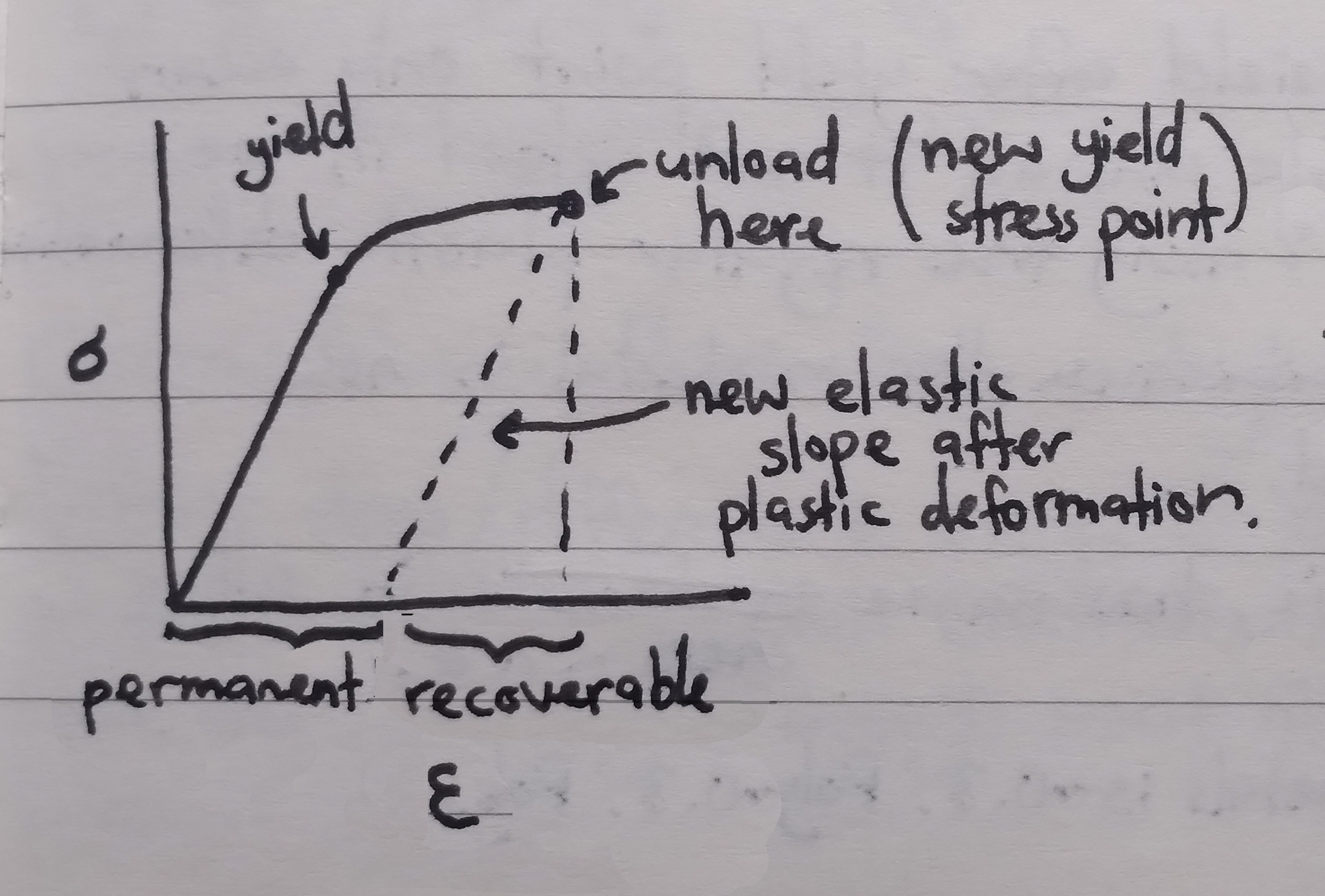
Continuing to strain the material past the yield point will ‘work harden’ the material (yield strength of a material increases with plastic deformation). If stress is removed after this point, the graph will descend with gradient E as the elastic portion of deformation is recovered. The point at which stress was removed is the new yield point of the material, and the distance between the original L_0 and the new length at rest measures permanent deformation. The curve will continue along the original trajectory once stress is reapplied.
Discontinuous yield is a phenomenon where the curve directly following the yield point is generally flattish with a lot of random noise. After this point the curve will become smooth again, even after the material is unloaded and reloaded. We’re told that this is (somewhat) unique to mild steel.
The stress at the peak of the curve is called the ultimate tensile stress, or UTS. Necking (localised reduction in cross-sectional area) occurs past this point up until fracture. This explains the downwards slope past the UTS, where the reduction in cross-sectional area leads to an increase in strain (due to the Poisson effect).
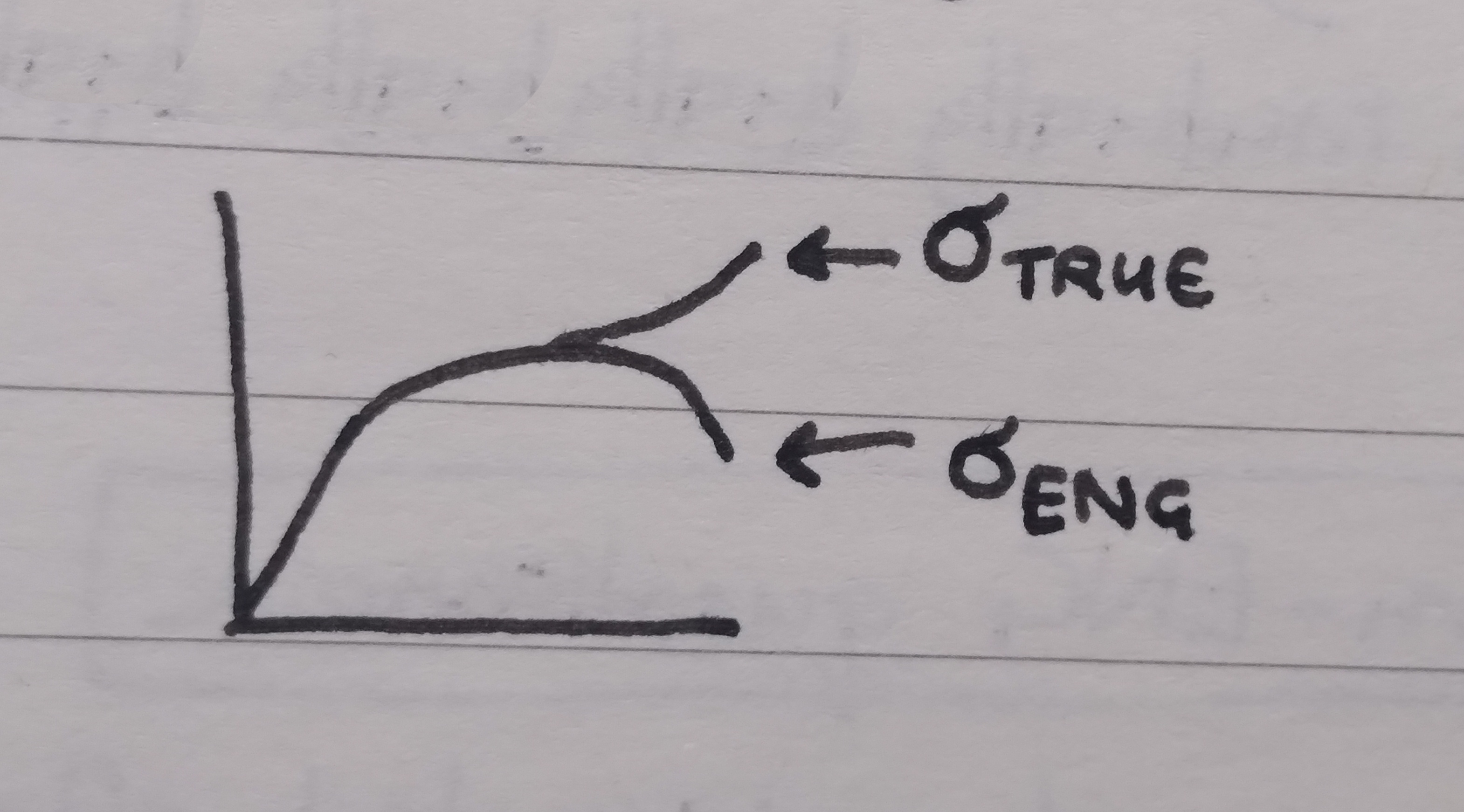
Since the stress on the graph is taken from the original cross-sectional area (engineering stress) there appears to be a reduction in stress after UTS, when in reality the reduction in cross-sectional area and continued increase in force would lead to an increase in stress.
Stress-strain curves show engineering stress, calculated from the original cross-sectional area of the material. In contrast, true stress is calculated from the real cross-sectional area (which changes continuously during the test). Engineering stress is used because it’s simpler to calculate, and because engineering projects will never come close to exceeding the yield stress of a material anyway (as this would permanently damage the material, impacting the integrity of the project).
Crystallinity refers to the degree of long-range structural order in the atoms of a material. A crystal lattice structure has atoms arranged in regular repeating patterns. Solid metals tend to be crystalline solids.
We can represent a crystal lattice using a unit cell, the smallest tileable portion of the lattice.
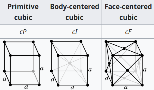
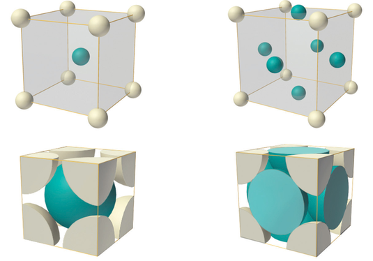
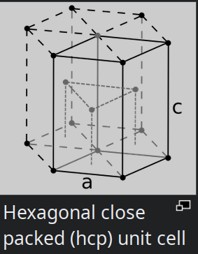
The three most common unit cells for metals are the body-centered cubic (BCC), face-centered cubic (FCC), and hexagonal close packed (HCP). FCC and HCP are close-packed structures, because they have the greatest possible atomic packing factor.
Polymorphic materials can exist in more than one structure. Iron is BCC at room temperature, but FCC at temperatures exceeding 912°C.
BCC
FCC
HCP
Atoms per cell
2
4
6
Coordination number
8
12
12
Unit cell dimensions
\frac{4R}{\sqrt{3}}
\frac{4R}{\sqrt{2}}
--
Atomic packing factor
68%
74%
74%
Examples
Cr, Mo, Fe
Cu, Al, Au
Mg, Ti, Zn
Physical properties
Brittle
Ductile
Very brittle
Atoms per cell The (fractional) number of atoms contained in the cell.
Coordination number the number of atoms bonded to any given atom in the lattice.
Unit cell dimensions Edge length a of the unit cell relative to the radius R of the atoms. To calculate, choose a close-packed vector in the cell, count the number of radii along that edge and divide by the edge length (a\sqrt{2} for a planar diagonal, a\sqrt{3} for a cubic diagonal).
Atomic packing factor The spherical packing ratio, given by the total atom volume over the cell volume, or atoms per cell times \frac{4}{3}\pi R^3 over a^3.
Ceramics are crystalline solids consisting of both metallic and non-metallic atoms and joined by a combination of ionic and covalent bonds. The crystalline structure is determined by the balance of charges (the resulting solid is electrically neutral) and by the relative sizes of ions (cations are positive and small, anions are negative and large). Cations can only bond with anions.
The two crystalline structures we’re looking at for ceramics are the rock salt structure (used by MgO, FeO, NaCl) and the silicate structure (used by rock, soil, clay, sand).
In the rock salt structure, each of the two atoms forms a separate face-centered cubic lattice, with the two lattices inter-penetrating to form a three-dimensional checker pattern. The interstitial sites of one lattice are filled with the atoms of the other. Coordination number is 6 (each cation only touches six anions, along cardinal directions), unit cell dimension in a = 2(R_a + R_c). Materials are thermally and electrically insulating, we’re told that this is due to a lack of free electrons.
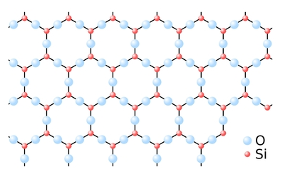
The silicate structure is based on the \ce{SiO4^{4-}} tetrahedra (\ce{Si} cation is +4, \ce{O} anions are -2). \ce{SiO4^{4-}} is not stable, but multiple of them can link together into a crystal lattice and sharing oxygen atoms (called ‘bridging oxygens’) to create \ce{SiO2} (silicon dioxide / silica), which has a neutral charge. Examples are quartz and amethyst (quartz with iron impurities).
Glass is an example of an amorphous silicate. Whether a silicate structure becomes crystalline or glass depends on how fast it cools from the liquid state. Rapid cooling doesn’t give the atoms time to arrange into a stable lattice, and so creates glass.
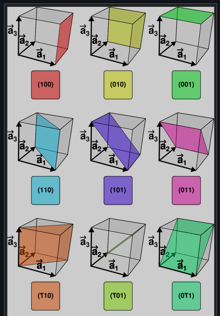
Miller indices describe how a plane intersects a unit cell. Each index is the reciprocal of the distance along a given axis, measured from the origin to the point where the plane intersects that axis. An index of 0 means that the plane runs parallel to that axis, 1 means that the intersection is at the far edge of the cell, and 2 means that the intersection is halfway along the cell (and also at the far edge). Planes repeat on a period of 1, so a negative index has the effect of reflecting the plane left-to-right along that axis (across the plane which bisects that axis in the cell).
Planes are denoted (h\ k\ l). Families of planes are denoted \{h\ k\ l\}, containing all planes which can be transformed into (h\ k\ l) by a symmetry operation that would leave the crystal unchanged (the planes are called ‘crystallographically equivalent’). Since we’re working with cubic cells, this includes any combination of reflections in all three axial planes. Specifically, for a cubic crystal, we just need to find all permutations of the three indices, including a positive and negative version of each index. The family \{1\ 1\ 0\} includes the 12 planes \{\pm 1, \pm 1, 0\}, \{\pm 1, 0, \pm 1\}, \{0, \pm 1, \pm 1\}. For lattices with lower symmetry, the planes in the family would be more constrained.
A similar notation is used for describing a ‘direction’ inside a unit cell (essentially a vector). Each index gives the distance along an axis from an origin where the direction intersects with the bounds of the cell, where 0 means that the direction is perpendicular to that axis. Indices are conventionally scaled to be integers (in other words, such that the greatest common divisor is 1), so the direction [1\ 0\ \frac{1}{2}] would become [2\ 0\ 1].
Directions within a cell are denoted [u\ v\ w]. Families of directions are denoted ⟨u\ v\ w⟩, containing all crystallographically equivalent directions in the same way as for planes.
Negative indices are denoted with an overbar, as in \{\bar{1}\ 0\ 1\}.
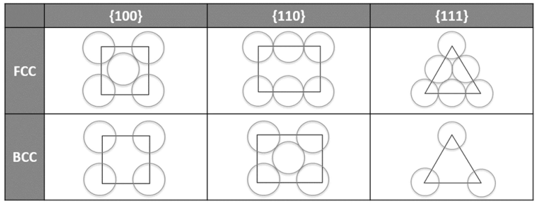
We can draw how a plane intersects with a unit cell in order to see how closely-packed the cell is along that plane. Only draw atoms where the center lies on that plane. The close-packed directions within that plane are those where the atoms are touching all along the line. A close-packed plane is one where all directions are close-packed, or in other words, where there is no gap between adjacent atoms.
If the atomic arrangement is the same on multiple planes, those planes are crystallographically equivalent.
In FCC, \{1\ 0\ 0\} is close-packed in ⟨1\ 1\ 0⟩ directions. In BCC, \{1\ 1\ 0\} is most closely packed in ⟨1\ 1\ 1⟩ directions, but doesn’t have a true close-packed plane.
During elastic deformation, the bonds between atoms stretch without breaking. This is analogous to spring deformation. The Young’s modulus E is an innate property of the material.
During plastic deformation, the bonds between atoms break and the planes in the lattice slide across one another, settling and re-bonding at the next closest stable position (this is easier in metals because there are a lot of free electrons). This is called slip. The model of slip that we use in this course is called box slip, where we look at unit cells in the lattice as cubes in a grid. In order for block slip to occur, every atom on the plane has to break and slip simultaneously, which requires a lot of energy.
On a close-packed plane, the distance to the next stable position is small, so the amount of energy/work (and therefore force) required to slip is small. This results in a weaker, more ductile material along that plane. In comparison, non-close-packed planes result in stronger, more brittle materials along that plane. This means that FCC materials tend to be more ductile, and BCC materials tend to be more brittle. An HCP structure has all close-packed planes lying in one orientation, so HCP materials are very strong and brittle (slip is very difficult).
The main slip system of a lattice is the planes and directions in which slip (and therefore deformation) can most easily occur (these are the closest-packed planes and directions).
The main slip system of an FCC lattice is \{1\ 1\ 1\}\ ⟨1\ 1\ 0⟩.
The main slip system of a BCC lattice is \{1\ 1\ 0\}\ ⟨1\ 1\ 1⟩.
For rock-salt structures, plastic deformation will cause cations to move to be adjacent to other cations, causing planes to repulse one another and the material to fracture. Plastic deformation of this structure is improbable.
The theoretical shear strength of pure elemental iron (based on the energy required to break bonds) is 10,000\unit{MPa}, but in practice the strength is only around 20\unit{MPa}. This is due to defects in the material.
One dimensional defects / point defects:
Vacancies An atom is missing from the crystal lattice, leaving an unfilled gap.
Substitutional atoms An atom is replaced with an atom of a different element in the lattice.
Interstitial atoms A smaller atom of another element is jammed into the interstitial space of a lattice.
Two dimensional defects / planar defects:
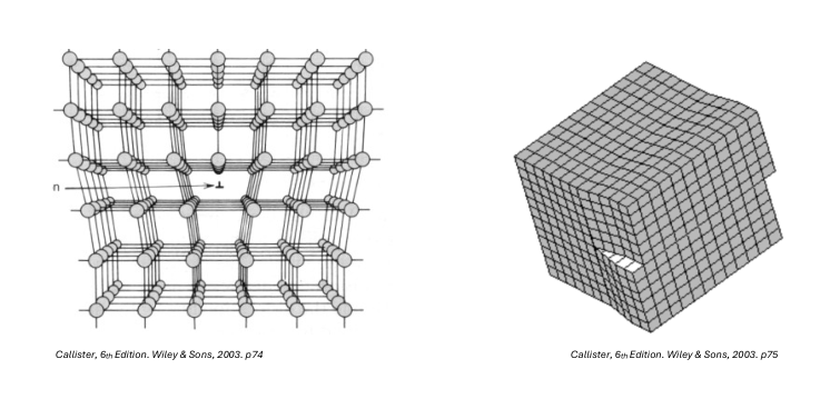
Edge dislocation An extra half-plane is inserted into the lattice.
Screw dislocation The lattice splits and twists such that the top and bottom interfaces of the split no longer align.
Dislocations in a lattice (notated as \perp) reduce the amount of energy required to slip because there are now fewer atoms on the plane, meaning that fewer bonds need to break before slip can occur. Less work is required to slip, corresponding directly to a lower yield strength for the material. Slip happens most easily on close-packed planes in close-packed directions.
Dislocations cannot occur in ceramics due to the strict structure enforced by bonds between cations and anions.
Resistivity \rho is a property that affects how easily electrons can move through a material. The resistivity of a material depends on its crystal structure.
\rho = \frac{R \x A}{l}
Conductivity \sigma is the reciprocal of resistivity. It shares the same symbol as stress, which is a little confusing.
\sigma = \1{\rho}
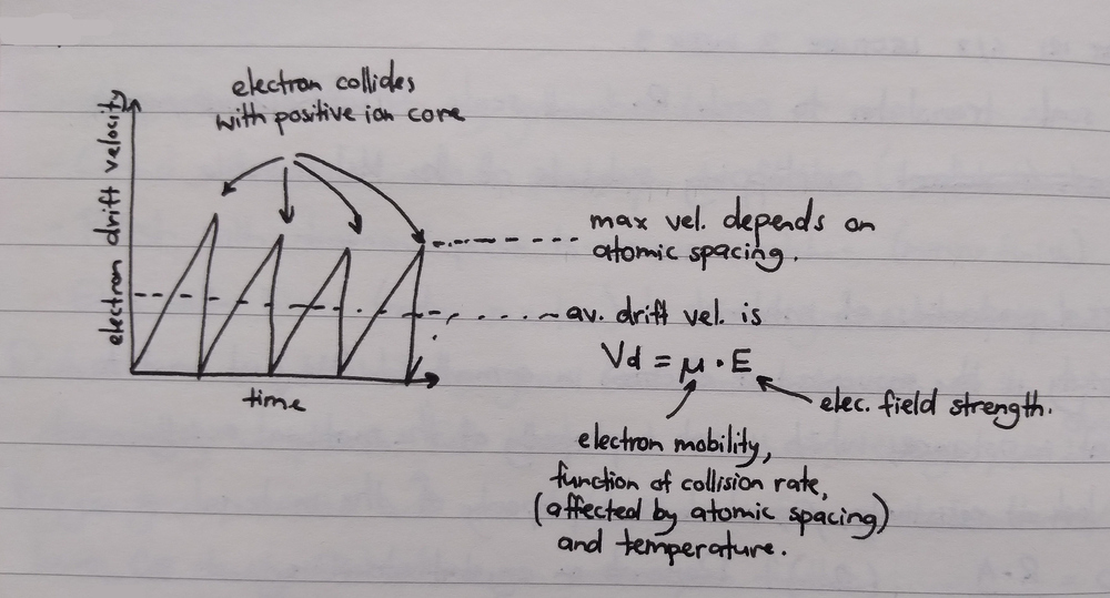
Metallic crystal lattices are formed from a lattice of positive ion cores surrounded by a cloud of de-localised electrons that can move freely through the lattice. When a potential difference is placed across the lattice, these free valence electrons ratchet from ion core to ion core, moving constantly towards the higher potential. As these electrons travel, they accelerate and then collide with the next ion core, increasing in velocity only to crash into the core and become stationary again (losing energy and generating heat). The electrons don’t hit every ion core along the path: if the temperature of the material is lower, the ion cores will vibrate slower, and there will be less chance that a given ion core will jump into the travel path.
The velocity of an electron moving through a metallic lattice can be modelled as a saw-wave graph, mapping electron drift velocity to time. Peaks on the graph indicate maximum electron velocity. Average drift velocity V_d is given by electron mobility \mu (a function of collision rate, affected by atomic spacing and temperature) and electric field strength E:
V_d = \mu \x E
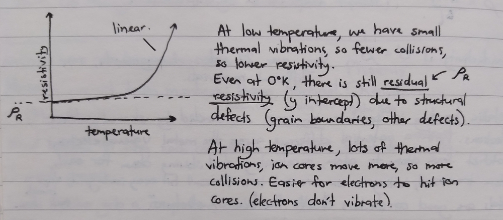
Resistivity is non-linear with temperature.
\rho_T = \rho_{0°C} (1 + \alpha_T \x T)
The resistivity of metals increases (possibly linearly) as the percentage of cold work increases (as this increases the number of dislocations in the material).
Ceramics and glasses are very good insulators. There is no ‘sea of electrons’, all electrons in the lattice are tied up in covalent and ionic bonds.
Most metals are crystalline, but instead of being formed from a single coherent lattice (monocrystalline), they tend to be formed from many smaller interlocking lattices of different orientations (polycrystalline). These individual lattices are called grains. Grains that are roughly spherical in shape are ‘equiax’, and grains that are longer and narrower are ‘elongated’.
Metallography is the process of grinding, polishing, and etching a polycrystalline sample in order to reveal the grain structure. The process is as follows:
Slice a thin sample of the material, embedding it into a lump of epoxy resin for easy handling.
Grind with silicon carbide sandpaper to flatten the surface (creating a scratched surface)
Polish with diamond paste to remove scratches (creating a mirror finish)
Etch with an acid or alkali to selectively corrode grain boundaries (we used 3% Nital, nitric acid in ethanol). This corrodes the grain boundaries with a redox reaction, reducing their reflectance.
The individual grains can now be distinguished under a microscope.
Grains form when a metal is cooled from a molten state (amorphous, atoms moving freely past one another) to a solid state (atoms lock in place). As the metal begins to cool, some atoms cling to one another to form nuclei crystals, and as the metal cools further these crystals attract more atoms towards themselves, eventually forming a voronoi pattern of grains.
Grain nucleation falls into two categories. Homogeneous nucleation is where atoms cling spontaneously to one another in the molten material, forming the basis for a spherical grain. This is very rare. Heterogeneous nucleation is where atoms nucleate on a surface (called a mould), creating a flat grain spread across the surface, or nucleate on an atom of a different element. This is far more common (we’re told it has something to do with thermodynamics).
Grain boundaries are a form of imperfection. Atoms inside a grain are called bulk atoms, and atoms at a grain boundary are called surface atoms. All of the bonds of a bulk atom are fully formed (linked into the lattice on all sides), but a surface atom has ‘free’ bonds. This makes a grain boundary a high-energy region due to these free atomic bonds, which are then able to bond with other atoms to reach a lower energy state.
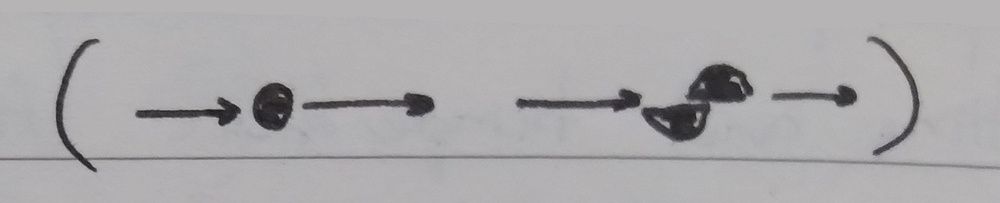
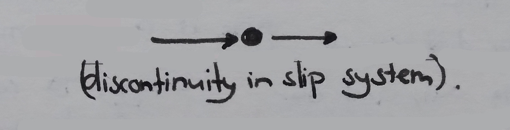
Grain boundaries inhibit the movement of dislocations because the lattices on each side of the boundary are discontinuous (‘discontinuity in planes’). Materials with many smaller grains are strong and brittle (‘higher grain boundary density’), and materials with fewer larger grains are weak and ductile (dislocations can move much further).
The Hall-Petch equation describes the relation between grain size and the yield strength of a material (I think it only applies to materials with equiax grains). \sigma_0 is the friction stress, the minimum stress required for dislocation movement to occur (or resistance of the lattice to dislocation motion), k is the strengthening coefficient or Hall-Petch constant, and d is the average grain diameter in millimetres. \sigma_0 and k are specific to each material.
\sigma_y = \sigma_0 + \frac{k}{\sqrt{d}}
When graphed, the x axis is \frac{1}{\sqrt{d}} (ranging from 0 to 0.3, smaller grains to the right), and the y axis is \sigma_y, with \sigma_0 being the y intercept. The gradient of the line is k and is positive. If we get smaller grains, we get an increase in yield stress.
Grains don’t form consistently through a material as it cools from molten to solid, because of the higher incidence of heterogeneous over homogeneous nucleation, and because the container that molten metal is poured into tends to be cooler than the metal itself. This means that most grains will form initially at the interface between the molten metal and the container.
An example used in class was the cross-section of a cast aluminium cylinder. To prepare the sample, molten 99.5% aluminium at 720°C (60°C above melting point) was poured into a mould made of 1” steel plate at room temperature and left to cool.
Initially, small equiax grains started to form on the mould walls due to heterogeneous nucleation (these grains are called chill crystals).
Next, columnar grains extended from the equiax grains, pointing towards the center of the mould.
Finally, larger equiax grains formed in the center of the sample, occupying roughly 50% of the cross-sectional surface area.
The aluminium contracted as it cooled, creating a large depression in what was the top surface.
There are multiple situations that can occur after the formation of columnar grains along the sample edges:
Equiax grains form in the center, bounded by the walls of columnar grains (most desirable outcome)
The walls of columnar grains keep extending until they meet in the center
Holes or pores form in the center (least desirable outcome)
Dendrites (columnar grains branch into tree structures) are formed
All of these situations are still non-optimal because the columnar grains make for an anisotropic material (a material that has different behaviour along different planes). What we most want is an isotropic material, one consisting entirely of equiax grains. This can be achieved by annealing the metal (heating then controlled cooling) or by using grain refiners (sprinkling Ti or Cd into Al to act as nucleation sites).
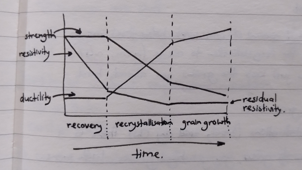
Annealing is a heat treatment that completely regenerates grains which have been deformed by cold work. This is useful for copper wiring for example, which is made brittle and resistive by the drawing process. Annealing transforms the strained longitudinal grains back into relaxed equiax grains, restoring ductility and conductivity. Annealing is generally performed at two-thirds of the melting point of the metal.
There are three stages to the annealing process:
Recovery Dislocations rearrange into a lower energy configuration, spreading out more evenly. Grains stay the same shape, the number of dislocations in the material stays the same, but the material does soften a little.
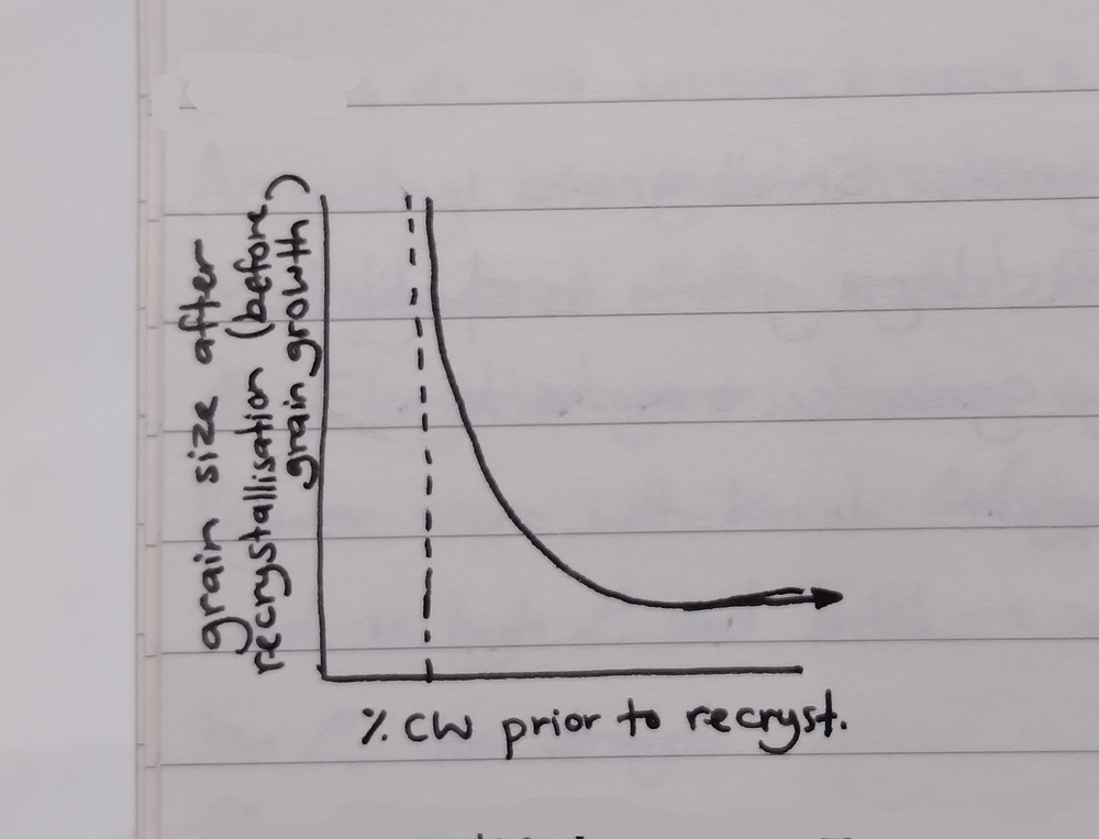
Recrystallisation New grains nucleate at grain boundaries (which are high energy sites) by consuming stored strain energy. These nuclei will then increase in size by cannibalising atoms from the neighbouring elongated grains, eventually replacing those grains completely with new equiaxed grains with low dislocation density / internal stress. If the material hasn’t been sufficiently cold-worked prior to annealing (called the ‘critical cold work’, normally around 4\%), then there won’t be enough stored strain energy to nucleate these new grains and kick off the recrystallisation process. The more cold work is performed prior to annealing, the greater the number of grains that will be able to nucleate, and the more and smaller the resultant equiaxed grains will be (because there will be less room to grow). The material will also be stronger as per Hall-Petch.
Grain growth If the material is kept hot following complete recrystallisation, the grains will continue to grow and cannibalise each other to a point, resulting in a coarser grain structure (fewer grain boundaries is a lower-energy state).
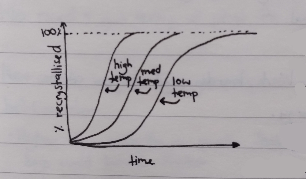
The recrystallisation temperature of a material is the temperature at which a 50\% cold-worked sample will fully recrystallise in exactly one hour. If the percentage of cold work is lower, the recrystallisation temperature will be higher, and vice versa. This is an intrinsic property of the material. The table below is given in °C.
Metal
Melt
Recrys.
Lead
327
-4
Aluminium
660
80
Copper
1085
120
Iron
1538
370
When a material is hot-worked (worked above the recrystallisation temperature), it will continuously recrystallise while you work-harden it.
When a polycrystalline material is plastically deformed, the individual grains will also become deformed. Running a material through rollers will flatten equiax grains into elongated grains. The grain volumes do not change.
When dislocations start slipping, we get also get multiplication of dislocations. Dislocations initially allow materials to slip easier, but each movement significantly increases the number of dislocations in the material and this acts to prevent the movement of other dislocations (because dislocations are planar discontinuities). The strength of the material increases until it loses the requisite ductility and the material fractures. There are also diminishing returns when using cold work to increase the hardness of a material — once the material is saturated with dislocations, adding more won’t meaningfully increase the hardness.
Cold work is where a material is plastically deformed at a temperature below its recrystallisation temperature. The amount of cold work experienced is given as a percentage (‘percentage of cold work’). This can be measured either as a change in thickness (when rolling a material) or a change in cross-sectional area (when drawing a material). t_0 is the original thickness, t_f is the final thickness, and then the equivalent for cross-sectional area. These equations rely on the assumption that the width of the material doesn’t change much.
Atoms move within a solid crystal lattice via solid state diffusion (as opposed to liquid state diffusion). Solid state diffusion can be by vacancy diffusion, where a vacant site moves across a lattice, or by interstitial diffusion, where small atoms move through interstitial spaces in the lattice (there might be other forms too). Diffusion is modelled as a random walk.
Solid-state diffusion is prevented by an energy barrier Q (called the activation energy), which is normally provided in the form of heat. The atom (or vacancy) will then move to the next stable position in the lattice. Solid-state diffusion is normally really, really slow, but increases exponentially with heat.
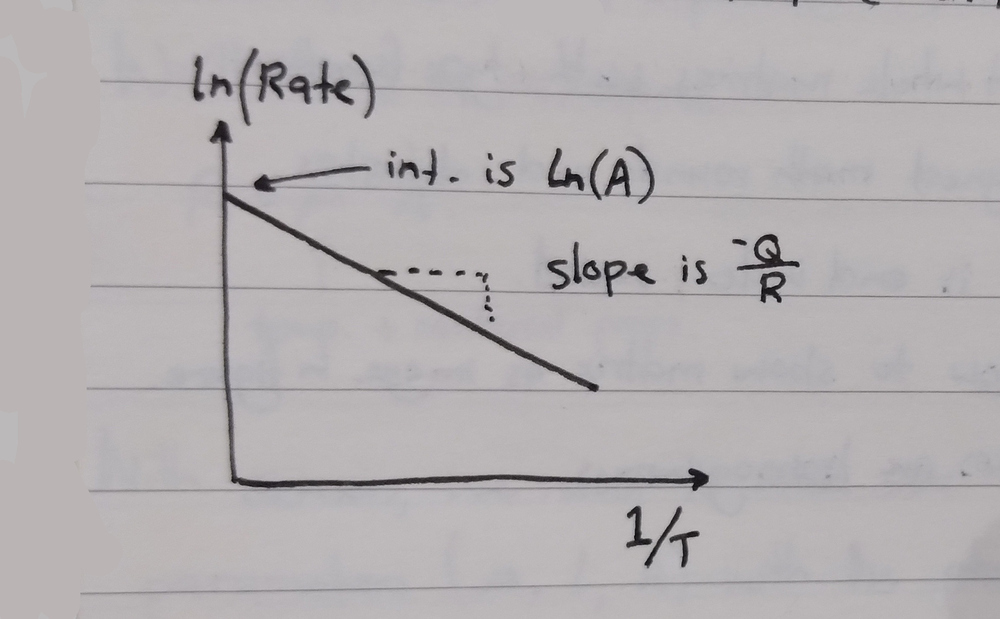
The Arrhenius equation models the diffusion coefficient D (rate of diffusion, given in \m^2/\s) given by a constant D_0, the activation energy Q (in \unit{J}/\unit{mol}), the gas constant R (8.314 \unit{J}/\unit{mol}\x\unit{K}), and the absolute temperature T (in kelvins).
D = D_0 \exp \left( \frac{-Q}{RT} \right)
This is plotted with \frac{1}{T} on the x-axis and with \ln(D) on the y-axis. This is because D increases exponentially as the reciprocal of temperature increases, so plotting in this way gives a straight line graph where the y-intercept is \ln(D_0) and the slope is \frac{-Q}{R}.
When salt is dissolved in water, we get a phase change. The water breaks the ionic bonds in the salt, creating a one-phase solution of salt (the solute) in water (the solvent). The salt solution saturates past a certain point, meaning that the water cannot dissolve any more salt, and you get salt precipitating on the bottom (a second phase, solid).
A phase is a “component within a system that has uniform physical characteristics”. The boundary between two phases is a phase boundary.
A solid is able to dissolve in another solid via solid-state diffusion. If both solids are metals, we call the resultant solution an alloy. An interstitial solid solution results from having tiny atoms dissolve in a matrix of larger atoms (such as carbon in steel). A substitutional solid solution results from having atoms replace other atoms of a similar size in a matrix (such as nickel in copper).
Solid solubility can be limited, where the parent matrix can only accept a certain percentage of solute before it saturates, or unlimited, where any proportion of either metal is possible. Interstitial solid solubility is always limited (C-Fe), substitutional solid solubility can be either limited (Cu-Ag) or unlimited (Cu-Ni).
A phase diagram shows which phases exist at equilibrium for various compositions and temperatures of a binary alloy. A material is at equilibrium when the temperature is constant throughout the material and is only increasing or decreasing very slowly.
We can use the lever rule to find the percentages of each phase that exist in an alloy system at a given composition and temperature:
Draw a point at the given composition and temperature.
Extend a line horizontally to the left and to the right until each end hits a phase boundary. These phase boundaries will border regions of pure phase.
To find the proportion of the mixture that is in a given phase, take the length of the line on the opposite side of that phase over the full length of the line. For example, if the phase boundary on the left is the liquidus (marking the full melting point), take the length of the right-hand line segment (extending from the point to the solidus). This can be see intuitively by thinking of a situation where the point is almost at the liquidus, with 10% of the line extending to the liquidus and 90% extending to the solidus — we know that the mixture must be mostly liquid with very little solid, so the proportion of liquid is 90%.
To find the composition of each phase, look at the percentage of solute that exists at that temperature at each end of the line. If the line intercepted the liquidus at 20% solute, then of the 90% liquid phase in the mixture, 20% is solute and 80% (100-20) is solvent. If the line on the other side intercepted the solidus at 40% solute, then of the 10% solid phase in the mixture, 40% is solute and 60% is solvent.
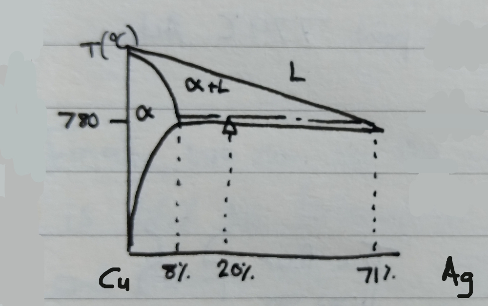
For example, if we have an Cu-Ag alloy at 780°C containing 20% Ag (as seen in the following phase diagram):
We measure a line to the left of our point, hitting the \alpha solidus, and to the right, hitting the liquidus.
The amount of solid \alpha phase in our alloy at this point is \frac{71-20}{71-8} = 81\%, and the amount of liquid phase is \frac{20-8}{71-8} = 19\%.
Of the 81% solid \alpha state, 8% is Ag and 92% is Cu. Of the 19% liquid state, 71% is Ag and 29% is Cu.
Bringing it all together, we can see that 81\% \times 8\% + 19\% \times 71\% = 20\%, which is the amount of Ag we started with.
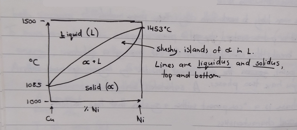
Binary isomorphous alloys are alloys of two elements with unlimited solid solubility. These alloys have two phases: a liquid phase, and a single solid phase \alpha. The atoms of the two metals are very similar in size — our example was Cu-Ni. The melting point of the alloy depends on the percentage of solute.
As the material cools, islands of solid \alpha form just below the liquidus, becoming big grains separated by small amounts of liquid just above the solidus, and then becoming a polycrystalline solid below the solidus.
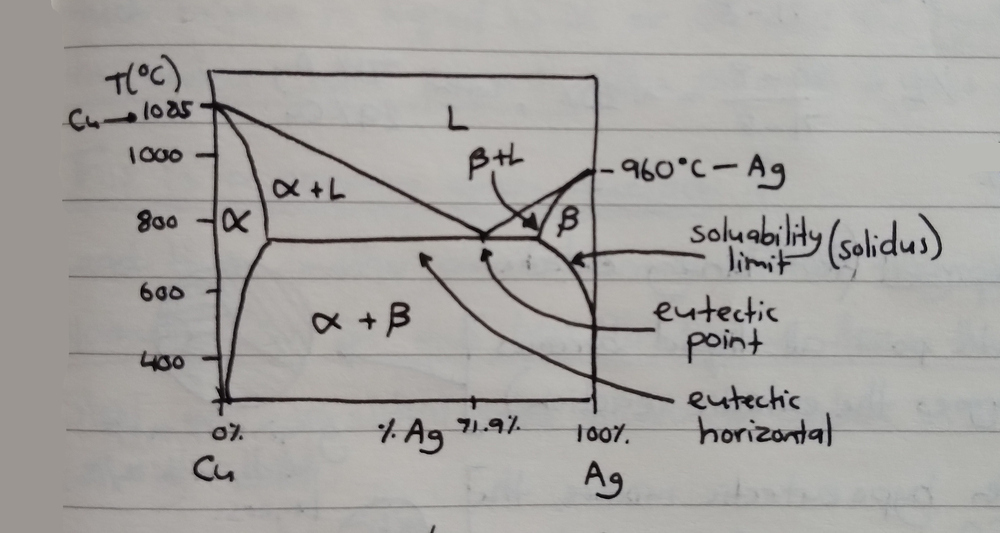
Binary eutectic alloys are alloys of two elements with limited solid solubility. These alloys have three phases: a liquid phase, a solid phase \alpha of majority one element, and a solid phase \beta of majority the other element. The atoms have a bit more of a size difference — our example was CuAg — such that only so much Ag (8%) can dissolve in Cu, and only so much Cu (8.8%) can dissolve in Ag. This solubility limit also changes with temperature.
Eutectic means ‘easily melted’. Binary eutectic alloys have a composition where cooling will transition directly from a liquid state to a solid state, with no intermediary ‘slushy state’ — this composition is called the eutectic composition (which depends on the alloy), and the exact transition point for this composition is called the eutectic point. The temperature that divides the liquid state from the solid states is called the eutectic temperature, or otherwise the eutectic horizontal.
When cooling below the eutectic temperature, the material undergoes the eutectic reaction, spontaneously forming finely interleaved layers of \alpha and \beta solid phases (a eutectic structure). This eutectic structure is very strong because of the very finely layered grain structure, which helps to block dislocation movement. The layers form through liquid-state diffusion.
The eutectic reaction occurs even if the mixture lies to the left (hypo-eutectic) or right (hyper-eutectic) of the eutectic point, because as the temperature cools towards the eutectic temperature, the excess Cu or Ag in the mixture sweat out into islands of pro-eutectic\alpha or \beta, leaving the liquid phase at exactly the eutectic composition by the time the mixture reaches the eutectic temperature.
The proportion of eutectic structure in a solid of a particular composition can only be calculated by looking at the phase percentages just above the eutectic temperature, because some of the \alpha or \beta in a a hypo- or hyper-eutectic composition will have gone towards pro-eutectic solid instead. The percentage of liquid state in the mixture will exactly equal the percentage of eutectic solid that will form.
If the composition instead causes the point to travel through the pure \alpha (or \beta) phases at either edge of the diagram, you’ll begin with 100% liquid phase, which cools into the pure \alpha region to become pure poly-crystalline \alpha. As it cools further, the solubility limit of the \alpha drops and the excess Ag sweats out to form new grains of \beta at grain boundaries.
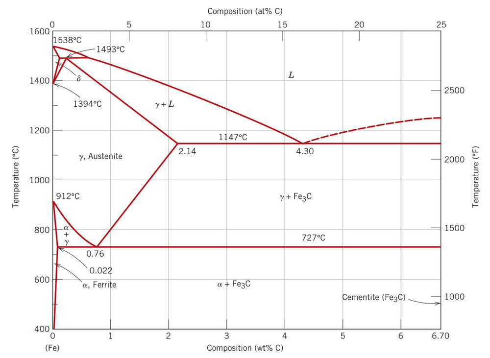
Steel is a very complex binary alloy (C-Fe). Carbon atoms are very small and can only slot into the interstitial spaces formed by the spherical packing of iron atoms. These interstitial spaces change dramatically when the iron lattice transitions from a BCC lattice to an FCC lattice above 723°C. The maximum solubility of C in Fe is 6.67%.
Steel can be categorised into ranges based on carbon content. Up to 0.25% C is called low carbon steel (also called mild steel), up to 0.5% C is called medium carbon steel, up to 0.95% C is called high carbon steel, and up to 4% C is called cast iron.
We care about three phases of steel:
\gamma — Austenite (gamma iron) FCC, holds up to 2.1% C. Exists above 723°C. Ductile, non-magnetic.
\alpha — Ferrite (alpha iron) BCC, holds up to 0.02% C. Magnetic.
\ce{Fe_3C} — Cementite (iron carbide) Ceramic, holds exactly 6.67% C. Very brittle (no slip systems).
Steel has both a eutectic temperature (at 1147°C) and a eutectoid temperature (at 727°C). The eutectoid temperature acts identically to the eutectic temperature from before.
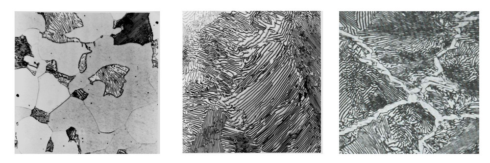
The eutectic structure of steel is called pearlite, which is formed from austenite (\gamma) of exactly 0.8% C composition. Pearlite is formed as interleaving thick layers of ferrite and thin layers of cementite. Unlike the eutectic structure, pearlite forms through solid-state diffusion, which is very slow, requiring very slow cooling. As before, we can have hypo- and hyper-eutectoid steels, and we can have chunks of pro-eutectoid \alpha or \ce{Fe_3C} in the mix forming at grain boundaries.
When eutectoid austenite (\gamma_{0.8}) is cooled slowly it forms coarse pearlite. The longer time spent at a higher temperature allows for greater solid-state diffusion, allowing the carbon atoms to move further and clump into thicker layers. When eutectoid austenite is cooled quickly it forms fine pearlite because the carbon atoms can’t move as far, forming closer layers. Fine pearlite is stronger and less ductile than coarse pearlite.
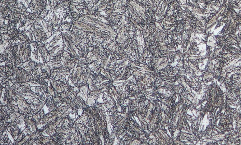
Cooling austenite rapidly through quenching creates martensite, a meta-stable phase of steel.
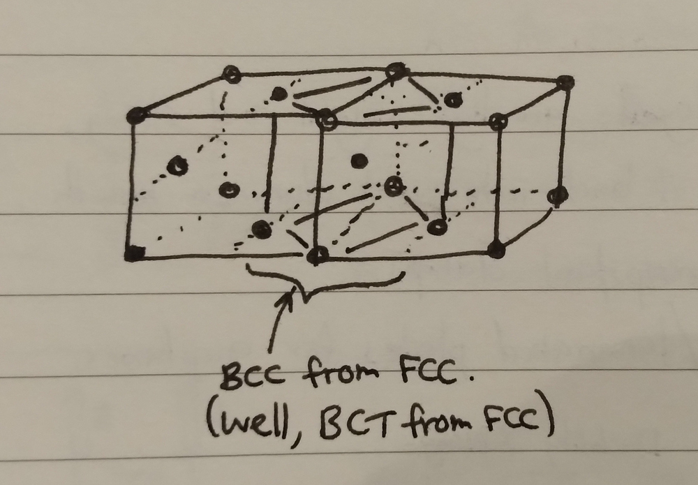
Normally, when austenite passes through the eutectoid temperature the iron lattice transitions from an FCC structure to BCC, with carbon solubility dropping from 2.1% to 0.02%. When quenching, however, there is no time for solid-state diffusion to occur, so the carbon atoms are trapped in place and the FCC structure changes instead to BCT (body-centered tetragonal, an elongated form of BCC). This is less of a change and more of a reinterpretation of the FCC structure (I don’t really understand this one). BCT has almost no slip systems and is extremely hard and brittle. The hardness of martensite increases with higher percentages of carbon (which creates lattice distortion, applying stress to the lattice).
Martensite is a dreadful material, it’s horribly brittle. It can be made much better through tempering (dispersion strengthening), dispersing fine \ce{Fe_3C} precipitates through the matrix. The martensite becomes \alpha + \ce{Fe_3C}, which is the same combination of phases as pearlite, but has quite a different structure. The BCT structure of martensite is only stable while carbon atoms are trapped inside it. When these carbon atoms diffuse out, the BCT \alpha_{ss} reverts to regular BCC \alpha. Tempered martensite has optimal strength with sufficient ductility for high toughness.
The properties of tempered martensite vary with the amount of time that the material is tempered for. As the material tempers, fine particulates will begin to clump (as per dispersion strengthening), leading to a more ductile material and less strong material.
Phase diagrams are only applicable when a material is at equilibrium, being heated or cooled extremely slowly. It can’t tell us what happens in a material as you heat or cool it more quickly.
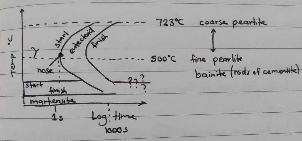
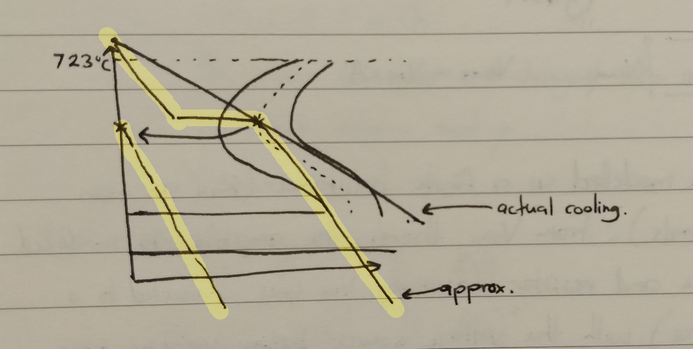
A TTT diagram allows us to see changes in a material of a fixed temperature over time (an isothermal transformation diagram). To use it correctly, you need to rapidly cool to a specific temperature and then hold there.
The swooping curve represents the zone at which pearlite is formed. The left-most point on the curve is called the nose, and it is at this point that fine pearlite is formed. At higher temperatures we get coarse pearlite, and at lower temperatures we get bainite, which is outside of the scope of this course. At much lower temperatures we get martensite. It takes about 1 second for pearlite to form; if we need more time, we can extend this out to about 20 minutes by alloying the steel with 1% Mg.
When continuous cooling is needed, a continuous cooling curve is used instead, but that’s outside of the scope of this course. We can, however, approximate continuous cooling with a TTT diagram.
We trace the actual temperature curve on the chart (seen below in yellow). In this example, we cool to around the nose point, forming fine pearlite. If we decide to continue cooling after the 50% pearlite mark, the composition of the material will be 50% pearlite and 50% austenite. We shift the cooling curve back to t=0 to see what happens with the austenite (the pearlite is already locked in), and we see that the curve plunges directly into the martensite zone without touching the eutectic curve, so we end up with 50% fine pearlite and 50% martensite.
Quenching steel can cause structural issues related to cooling speed. The surface of the steel cools much faster than the center, and as mentioned before the time taken for pearlite to begin to form is only 1 second, so a thick steel rod when quenched will become concentric layers of martensite, then bainite, and then fine and coarse pearlite.
As before, the addition of 1% Mg to the alloy will extend out this time period, allowing for a more consistent structure to form when quenched.
Spheroidising is a weakening mechanism. Slow-cooled high-carbon steels contain a lot of hard and brittle \ce{Fe_3C}, which wears out machining tools more quickly. To remedy this, the steel can be made temporarily soft and ductile while it’s being machined, and then heat-treated to make it hard again afterwards.
We can convert \ce{Fe_3C} layers in the steel into spheres by heating the material to around 700°C and holding it there for several hours, allowing for heavy diffusion of the carbon within the steel. These layers draw inwards, creating individual spheres dispersed throughout a ferrite matrix. A sphere has the highest volume to surface area ratio of any shape, so the surface area of \ce{Fe_3C} in the steel is reduced.
To revert the spheroidisation, the material is heated above the eutectoid temperature (forming austenite), and then cooled to form pearlite.
To strengthen any material, we’re really just looking to inhibit dislocation movements, preventing plastic deformation.
For pure metals and alloys:
Cold work Multiply the dislocations in a material through cold work (dislocations are inhibited by dislocations).
Hall-Petch Increase grain boundary density through cold work and annealing, making grains smaller (dislocations are inhibited by grain boundaries).
For alloys:
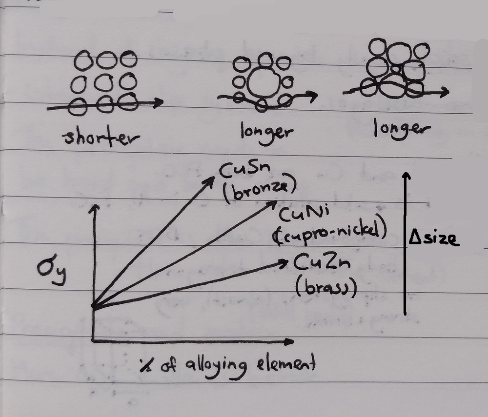
Lattice distortion Increase the equilibrium distance in the lattice by introducing atoms of much larger or smaller elements. These atoms have to stay in close contact with neighbouring atoms in the matrix, but the difference in sizes introduces distortion so that the path length through any one chain of atoms becomes longer.
Multiphase strengthening Increase phase boundary density through the eutectic/eutectoid reaction, creating fine layers of alternating phases (dislocations are inhibited by phase boundaries).
Dispersion strengthening Quench to form a super-saturated \alpha phase, then temper to finely disperse hard precipitates throughout the material (dislocations are inhibited by hard precipitates).
The larger the size difference between the atoms of the two elements, the greater the distortion of the lattice. The distance along each path / slip system in the lattice is increased by the distortion, which increases the equilibrium distance, which increases the yield strength of the material.
Dislocations are stopped by phase boundaries, similarly to with grain boundaries, so we can strengthen a material by increasing the density of phase boundaries through the eutectic/eutectoid reaction.
The example given to us in class was in the use of AlCu alloys for aircraft fuselages. AlCu is a binary eutectic alloy with two solid phases:
\alpha, a solid solution of Cu in Al. Both Al and Cu are FCC, so \alpha is also FCC. Ductile.
\theta, the compound \ce{CuAl_2}. This is BCT / body-centered tetragonal, an elongated form of BCC, which has almost no slip systems. Extremely strong and brittle.
To effectively strengthen this alloy through multiphase strengthening, we want an alloy of the eutectic composition, maximising the amount of eutectic solid that forms on cooling. If we fall on either side of the eutectic composition, we’ll end up with clumps of pro-eutectic \alpha or \theta which will allow much more dislocation movement than eutectic structure alone. Pro-eutectic \theta is very strong and brittle, which makes for a very unpredictable material. Pro-eutectic \alpha is very weak and ductile. Eutectic structure itself is quite strong and a little ductile.
Dispersion strengthening works by distributing small precipitates through the metal (the parent matrix), which act to interrupt slip systems. This is also called age hardening or precipitation hardening.
There are some restrictions before we can perform dispersion strengthening:
The phase diagram should exhibit decreasing solid solubility of the strengthening phase (\theta, the brittle phase) with decreasing temperature to allow super-saturation when quenching. This refers to the positive gradient of the \alpha boundary below the eutectic temperature on a binary eutectic phase diagram. An alloy where this isn’t the case is brass.
The parent matrix should be relatively soft and ductile to provide toughness, and the strengthening precipitate phase should be hard and brittle and finely dispersed to provide strength.
The alloy should be able to survive the quenching process (thermal shock will cause some materials to deform or fracture when quenched).
The precipitant should be:
hard and brittle, otherwise the precipitant will be sheared by applied forces
many and small, to better distribute through the material and lie in the way of any possible slip path (the center of a large precipitant is wasted, because dislocations are already stopped by the edges)
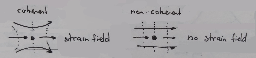
coherent with the parent matrix, in order to generate a strain field / lattice distortion, increasing the distance between equilibrium states and further increasing yield strength
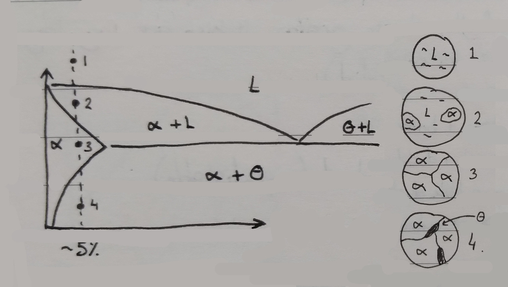
Dispersion strengthening is performed according to the following process (for an example hypo-eutectic AlCu alloy):
The material is heated to a point above the solidus, such that it consists entirely of polycrystalline \alpha.
The material is cooled rapidly (quenched), passing into the \alpha + \theta region of the phase diagram. Normally, the reduction in solid solubility at this point would cause \theta to sweat out, forming brittle grains at grain boundaries. However, the rapid cooling doesn’t allow time for solid-state diffusion to occur, and the excess Cu is trapped inside the \alpha state. This creates a super-saturated \alpha state (written \alpha_{ss}), which is meta-stable and stronger than regular \alpha (due to excess Cu). The \alpha_{ss} is a very high energy state in a local minima, remaining stable until a nudge of energy gives it the ability to finally shed the excess Cu, returning to a much lower energy \alpha state.
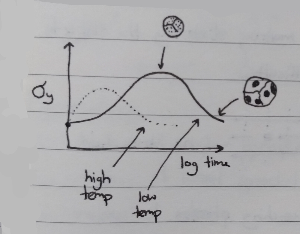
The material is heated to a point below the solidus to allow diffusion to finally occur. This would normally cause grain of \theta to form at grain boundaries (high-energy areas), but the \alpha_{ss} is much higher energy, so tiny grains of \theta form evenly throughout the material. This precipitation is caused by diffusion, and so is governed by time and temperature (as per Arrhenius).
The lower the diffusion temperature, the smaller the precipitants and the stronger the resultant material. We want to use lower temperatures and longer times (3 hours vs 20 minutes) in order to obtain the strongest possible material. After too long, solid-state diffusion causes the \theta precipitants to start to clump, reducing strength again. Precipitation doesn’t end once the material reaches room temperature either, diffusion slows but does not stop. This means that older alloy samples have a tendency to be stronger than newer samples (unless they make it past the hump, I guess).
Organic chemistry is the study of carbon-based molecules, which tend to contain a backbone of carbon atoms with hydrogens (or other atoms) bonded at the edges.
Molecules are named after a set of basic rules:
A prefix of meth/eth/prop/but/pent/hex/... indicates the number of carbon atoms along the central chain (1, 2, 3, ...)
A suffix of -ane/-ene/-yne/... indicates the maximum number of bonds between any two carbon atoms (single, double, triple, ...)
An additional -ol suffix indicates the presence of an oxygen-hydrogen pair.
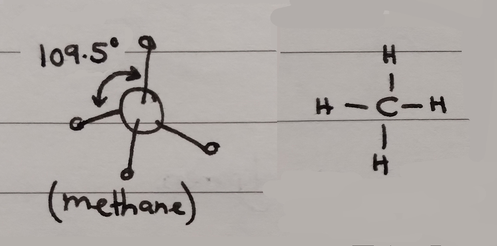
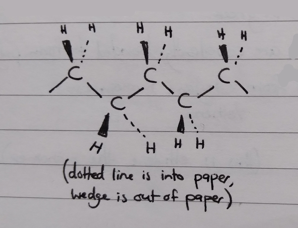
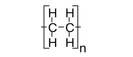
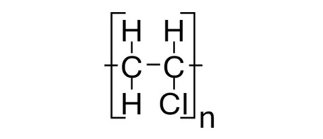
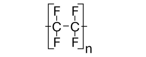
The simplest organic molecule is methane (\ce{CH_4}) which consists of a single carbon bonded to four hydrogens. Adding another carbon gives ethane, then propane, butane, etc. The angles between bonded hydrogens or carbons are a constant 109.5° due to Coulomb forces repelling adjacent atoms from each other. This angle causes the carbon-carbon backbone to form a permanent zig-zag shape, which makes polymer chains tangle and wrap around each other easily (bonds can rotate as long as the angle is preserved).
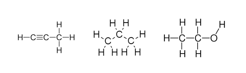
The molecules in the following picture are:
propyne (3 carbons, triple bond)
propane (3 carbons, single bond)
ethanol (2 carbons, single bond, with an oxygen-hydrogen pair)
Degree of polymerisation is a measure of the length of a polymer chain, as the number of monomer units making up the chain. Higher numbers represent longer chains, directly correlating with the mechanical properties of the material.
\text{DP} = \frac{\text{avg. molecular weight of polymer chains}}{\text{weight of a single monomer unit}}
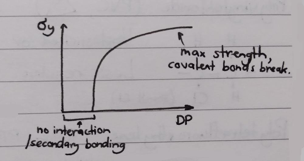
The degree of polymerisation directly correlates with yield strength:
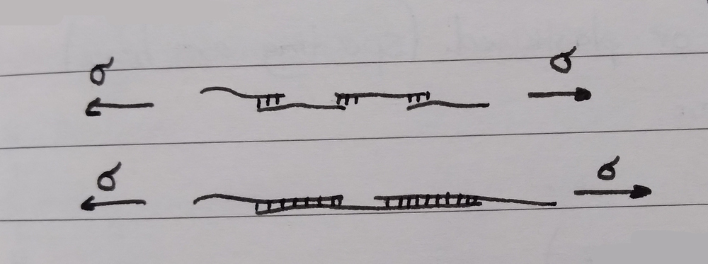
Polymers with a low degree of polymerisation (short chains) have few secondary bonds, which are easy to break or untangle (weak forces allow chains to slide against each another).
Polymers with a high degree of polymerisation (long chains) have lots of secondary bonds, making them very hard to break or untangle (high forces prevent chains from sliding against each other). Longer chains are also more likely to tangle in the first place.
With a sufficiently high applied force, the strength of the material comes entirely from the strength of the carbon-carbon backbone, not the intermolecular forces.
Linear polymers are formed from repeating monomer units arranged end-to-end with no branching. Chains are long and flexible, and the material can be high density / close-packed.
Branched polymers are formed from a main backbone with attached side branches. Branches prevent the chain from packing close, so the material is lower density.
Cross-linked polymers are formed when polymer chains are bonded together with short covalently-bonded segments, forming a strong mesh.
Thermoplastics (thermoplastic polymers) Polymers that soften with increasing temperature. They have either linear or branched structures, with weak secondary bonds. These secondary bonds are further weakened by the vibrations caused by heat, but will be restored once the material has cooled. This allows for the material to be reshaped repeatedly.
Thermosets (thermosetting polymers) Polymers that do not soften with heat. These are cross-linked polymers with strong covalent bonds. They are hard, strong, and insulating, they char instead of burning, and they can’t be recycled.
Elastomers (includes rubber) Polymers that can experience very large elastic deformations. These are formed from highly coiled polymer chains with a few covalently-bonded cross-links to prevent the chains from sliding (which would cause plastic deformation). There’s an optimal number of cross-links, too many makes for a hard rubber and too few makes for a weak rubber.
Polymer bulk structures range from amorphous to partially crystalline.
When amorphous, polymer chains are mixed with no long-range order. Chains form a squiggly noodly mess with no mechanical strength. Amorphous structures are completely transparent.
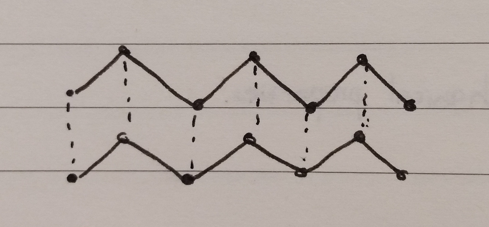
When partially crystalline, sections of polymer chains zig-zag against each other and form long-range order.