bedrock-micro is an emulator for the Bedrock computing system that runs on a $1.50 NZD microcontroller (the PIC12F1572). This project is currently in development, but low priority.
Overview
The purpose of this implementation is to run Bedrock on the most constrained system possible. Excluding the power supply, the core will run on two 8-pin chips costing a total of $4.90 NZD incl. GST (surface-mount), with a couple of logic chips on the side to implement multiplexing for the device bus.
I intend for this Bedrock implementation to not only be technically usable, but to actually be a genuinely productive system for hacking on. The circuitry should all fit on a board smaller than an eftpos card, powered by a button battery, and with sixteen tiny JST connectors for the device bus. A whole computer in your pocket, as it were.
Rough calculations indicate that the whole system will run at full throttle for 56 hours (2 days) on a single CR2032 button battery, or for 675 hours (28 days) on two AA batteries. This would be worst-case power consumption, where the Bedrock program is trapped in an infinite loop. The actual power consumption of the system is expected to be around 90% lower in practice.
The microcontroller
The PIC12F1572 is one of the lowest-end microcontrollers that money can buy. It boasts:
- 2048 words of read-only program memory
- 256 bytes of read-write register memory
- 128 bytes of non-volatile flash memory
- 16 levels of stack
- 8MHz instruction clock
The highest-frequency internal oscillator is 32MHz, but each instruction takes four clock cycles. - 6 input-output pins
- 49 instructions (depending how you group them)
- 2.5V to 5.5V input voltage range (with 32MHz clock)
- 2.1mA operating current (with 32MHz clock)
Power consumption at 3.3V and 32MHz is 6.9mW. - 0.3μA sleep current
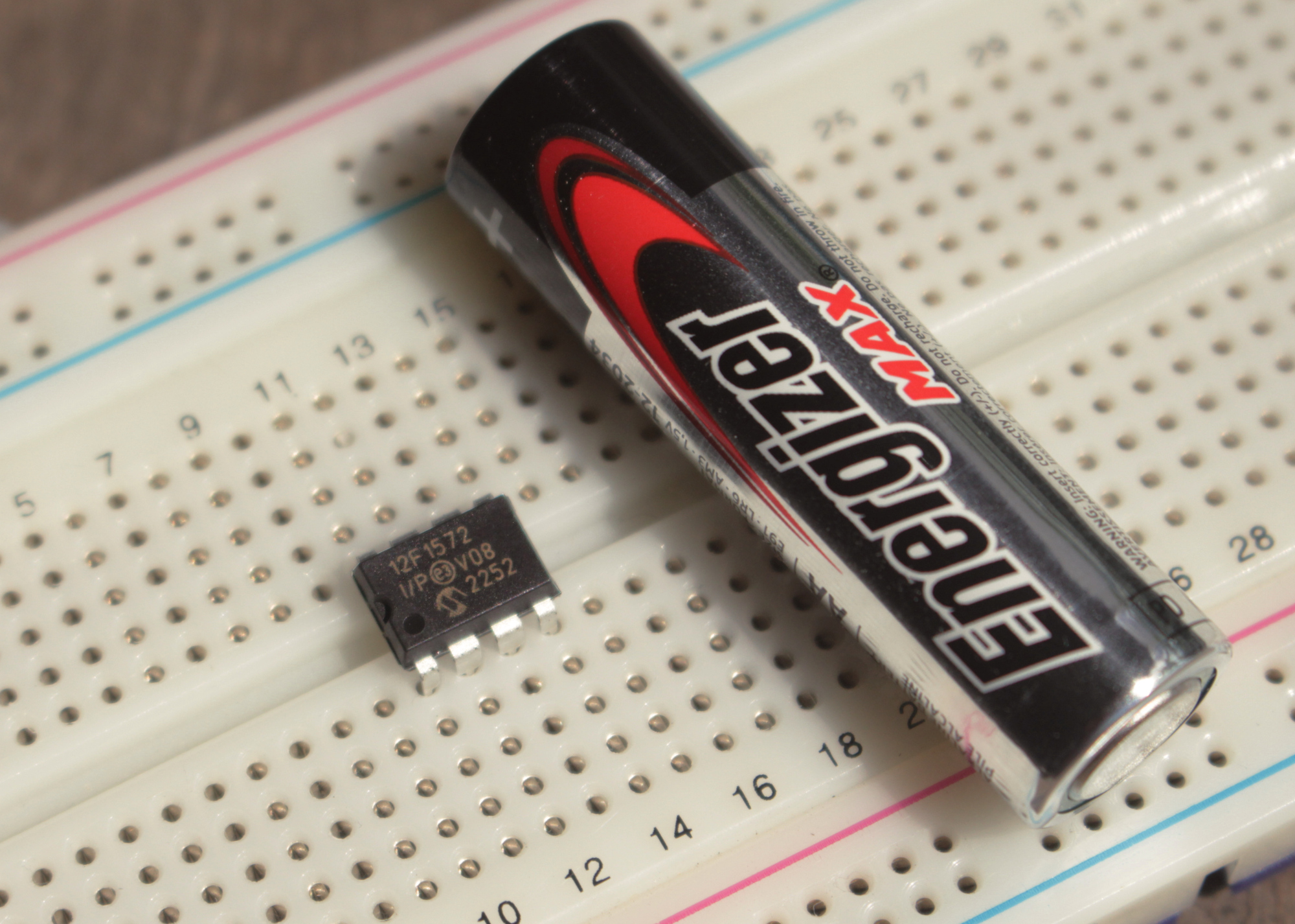
Here’s a photo of the DIP version of the chip ($1.95 NZD incl. GST from element14), with an AA battery for scale:
Implementation
Program memory
There is nowhere near enough memory on-chip to hold the currently-running Bedrock program, so we need an external memory chip. We’ll use the MCP23LC512, a 64KB SRAM chip that communicates using SPI. It has:
- 64KB of memory
- 2.5V to 5.5V input voltage range
- ~2mA operating current
- ~2μA standby current
The chip includes sequential read and write modes, allowing us to easily read consecutive instructions from memory or write a new program to memory with minimal overhead. The DIP version of the chip ($3.97 NZD incl. GST from element14) has the same footprint as the microcontroller.
We’ll keep the memory chip active all of the time, except when accesing a device. This will allow us to keep the sequential read active, meaning that we won’t have to regularly re-transmit the full instruction pointer address to the chip, we can just lean on sequential reads.
Stacks
The 256 bytes of read-write register memory on the microcontroller is organised into four blocks:
- Three 80-byte blocks spread across three banks
- One 16-byte block accessible from any bank
This would normally be a massive pain to work with, but the microcontroller also features two ‘indirect registers’ that act like pointers into memory. Importantly, these indirect registers can address the three 80-byte banks as a single 240-byte array, we just need to set the high byte of the 16-bit indirect address to 0x20 and the low byte to an array index (0x00 to 0xEF). We’ll reserve the second indirect register (called FSR1) for stack accesses so that we can set and forget that high byte.
So, we only have 240 bytes of memory available to us. We’ll be making a slight compromise here: each stack will get only 120 bytes of memory instead of the full 256 bytes requested by the Bedrock specification. This is fine in practice, 120 bytes is still an enormous amount of memory for a stack and is more than sufficient for every Bedrock program written to date. We could be tricky and have one stack grow from the left and the other from the right, but then we wouldn’t be able to take advantage of symmetry when accessing the stacks.
The base of the working stack will be 0x00, and the base of the return stack will be 0x78. There won’t be any guards in place to protect against underflow or overflow, we’ll just let the program do its thing.
Device bus
We’re already using three pins for SPI to communicate with the memory chip, so we’ll reuse them for the device bus as well. That brings us up to three pins for SPI (clock, data in, data out), one chip select pin for memory, and one chip select pin for the device bus.
When accessing a device, the microcontroller will activate the device bus chip select line (bringing it low), and then will pulse out a 12-bit command over SPI. The first four bits will be the slot number (activating a single device), followed by four bits for the port number (received by the device) and a four-bit command (also received by the device). The device only receives eight bits in all.
When a device is made active (after the first four bits are sent), the activated device will bring the microcontroller input line high to indicate that it’s still processing the request. After the command is sent, the microcontroller will wait until the line is brought low again, and then it will clock out the response byte (if any) or otherwise just continue. If the chip select line is disabled (brough high) before the response has been returned, the device will drop the whole response (so that the microcontroller can read just the first bit of the wake flag or connection state).
The following list contains the eight device commands. Every odd-numbered command returns a byte, every even-numbered command returns nothing. The remaining eight commands are reserved for device-specific functionality (could be useful for debugging).
0x00Check connection
Pings a slot, returning0xFFif a device is connected to that slot (or0x00otherwise).0x01Reset device
Reset the device (as per the fork port of the system device), returning nothing.0x02Read byte
Read a byte from a device port, returning the byte that was read.0x03Write byte
Write a byte to a device port, returning nothing. This command sends an additional 8 bits following the command.0x04Read wake flag
Clear the device wake flag, returning0xFFif the flag was previously set (or0x00otherwise).0x05Notify sleep
Sent when the system is put to sleep, returning nothing. This is used by a double-buffered screen device to trigger a buffer flip.0x06Get name byte
Return the next byte of the device name (as per the device name ports of the system device).0x07Reset name pointer
Reset the pointer that keeps track of the next byte of the device name (as per the device name ports of the system device).
In addition to the microcontroller and the memory chip, I’ll need a 74HC164 8-bit parallel-out shift register feeding into a 74HC154 4-to-16 inverting multiplexer in order to implement multiplexing for the device bus.
The microcontroller will implement the system device internally. I’m not sure how debug functionality will work, it’s important for the system state to be able to be sent to an external circuit for display, but also for all four custom devices to be available for use.
Devices will connect to the device bus using six-pin connectors. I’m looking into six-pin JST SH connectors at the moment for the final board, but the prototype will just use 6 header pins. The pins are:
- Power (3.3V, up to 20mA per device)
- Ground
- SPI data in
Controlled by the device, sending data from the device to the microcontroller (MISO). This pin is pulled high by the device when the chip select line becomes active, and is brought low again to signal to the microcontroller that the command has finished processing. - SPI data out (MOSI)
Controlled by the microcontroller, sending data from the microcontroller to the device (MOSI). - SPI clock
Controlled by the microcontroller. A bit of data is written to the device on the rising edge and read from the device on the falling edge. - SPI chip select
Controlled by the microcontroller, active low.
A benefit of using SPI as the communication protocol for devices is that it can be clocked by hand when testing out device circuits, you don’t need complex circuitry to transmit commands. It’s also just simpler to implement and more robust than something like I2C.
Power supply
If it’s not too expensive, I’d like to include a voltage regulator chip in the final design. This will most likely be the MCP1252-33X50, a buck/boost converter:
- 2.0V to 5.0V input voltage
- 3.3V or 5.0V selectable output voltage
- 80μA power consumption
- 120mA maximum output current
It’s only available as a surface-mount component, costing $4.03 NZD incl. GST from element14. This is almost the same price as the other two chips combined, which is inconvenient. It also requires three capacitors, which are $1.00 a piece. Cheaper capacitors might be available, especially surface-mount.
The plan, if I include the voltage regulator, is to include a button battery holder and a generic two-pin connector for an external battery, both feeding into the regulator. This would allow the system to run portably, but also to be connected to any other power source if the need arises.
Bootloader
The 128 bytes of non-volatile flash memory is going to hold the Bedrock bootloader program. This program will access the device bus to read a larger program from a pre-defined location on the file device, falling back to the stream device if the file device is not available.
Firmware
I’m writing the firmware for the microcontroller using Torque, everyone’s favourite meta-assembler.
The current in-progress firmware source file can be downloaded from bedrock-micro.tq.
Circuit design
Bill of materials
Integrated circuits:
PIC12F1572microcontrollerMCP23LC51264KB SRAMMCP1252-33X50voltage regulator
Requires three supporting capacitors.74HC1648-bit shift register74HC1544-to-16 inverting multiplexer
Connectors:
- 16x 6-pin JST SH sockets
For the device bus. - 1x 1μF capacitor
For the voltage regulator. - 2x 10μF capacitor
For the voltage regulator. - 1x CR2032 battery holder
GPIO allocation
We have exactly the right number of GPIOs available to us on the microcontroller:
GPIO 0SPI clock (output)GPIO 1Device address clock (output)GPIO 2SPI data out (output)GPIO 3SPI data in (input)GPIO 4Memory select (output)GPIO 5Data bus select (output)